Upload
Home
Manufacturing basics for microfluidic devices
By Joshua Gomes
A primer on the most common microfluidic fabrication methods.

Introduction link to Introduction section
Microfluidic technologies have led to game-changing advances in drug discovery, genomics, precision medicine, and diagnostics. However, a major hurdle in microfluidic development lies in the manufacturing of micro-scale devices. There are several different processes available with different strengths, weaknesses, and underlying principles that should be considered before choosing a strategy.
Microfeature forming methods
One of the core elements in microfluidic manufacturing is the process of forming the fluidic layer, or the body of the device, which contains the channels and microfeatures used to manipulate fluids. There are several manufacturing techniques to fabricate fluidic layers that can be broadly classified into Prototype processes and Production processes.
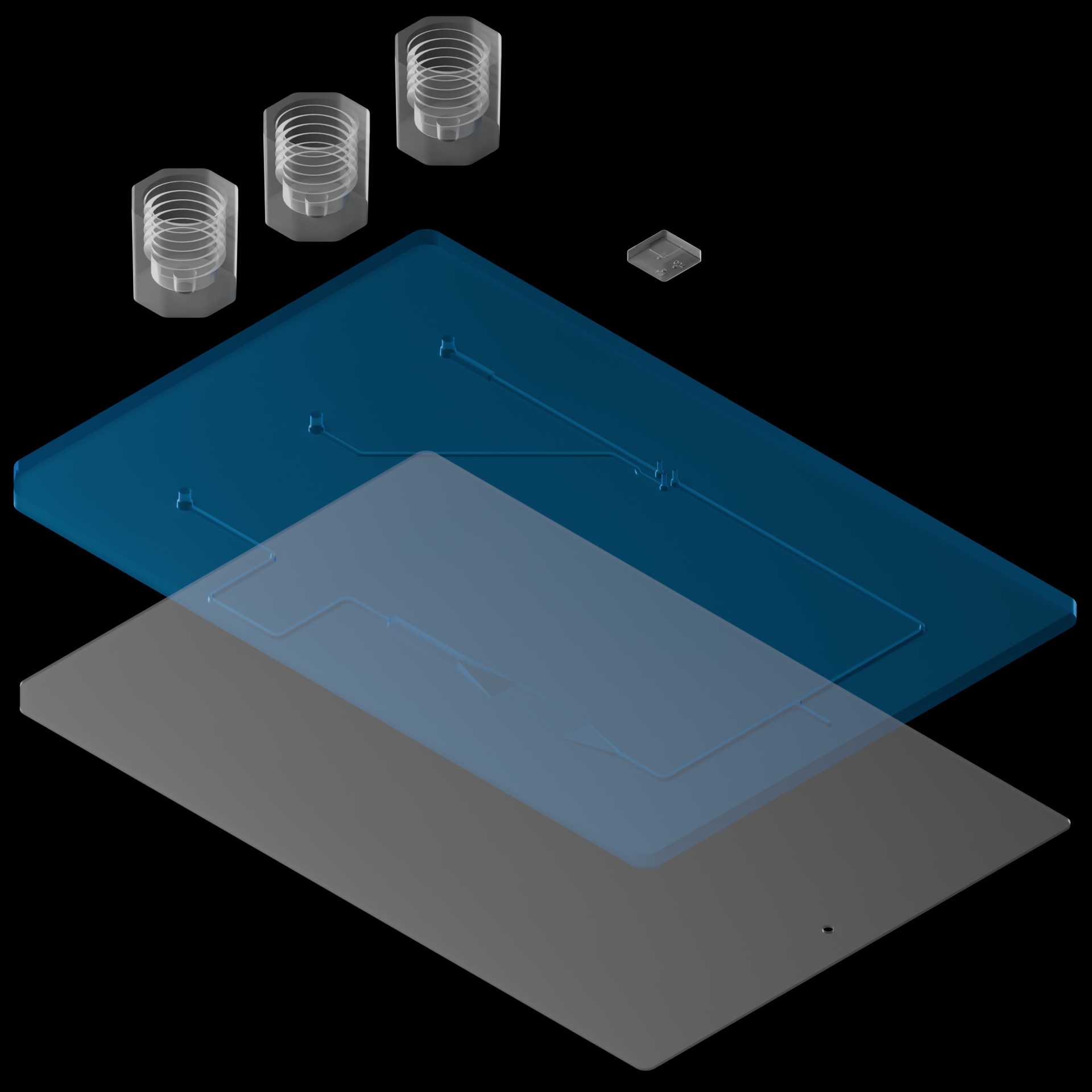
Exploded view
Prototype processes link to Prototype processes section
Polydimethylsiloxane (PDMS) casting
The most common prototyping technique used in academic research is to fabricate fluidic layers by casting uncured polydimethylsiloxane (PDMS), a clear silicone rubber, onto a mold. The cured rubber can then be removed, leaving the imprint of the microfeatures in the silicone rubber body. This technique is relatively low cost and can yield devices with impressive microfeature geometry and accuracy by using photolithography techniques to create the mold. Much of the early microfluidic research focused on PDMS devices, and thus it has become one of the most prolific prototyping methods in the industry. However, PDMS is a material with a few potentially problematic properties, including high gas permeability and absorption of small molecules. Also, it is a difficult manufacturing technique to transition to high-volume production.
Subtractive manufacturing
Alternatively, subtractive techniques can be used to form microfeatures in thermoplastics by removing material from a starting block or blank. Some examples of subtractive methods include micromilling and laser machining. Both techniques allow the use of thermoplastic materials, which are generally much more appropriate for high-volume manufacturing, but each has its own limitations. Milling channels and features below 200 microns in cross-section becomes quite difficult, and the rough surface finish and burrs leftover from the machining process can create challenges with flow and imaging properties. Laser machining is only compatible with a small subset of thermoplastics and can suffer from batch-to-batch repeatability issues and a lack of control in microfeature cross-section.
Additive manufacturing
Additive manufacturing via 3D printing has become extremely useful in many product development processes. But, in microfluidic projects, 3D printed prototypes are generally limited in resolution, have poor control over surfaces, and are made from materials with chemistries that can compromise assays and imaging methods. Like PDMS casting, 3D printing is also not a technique that effectively scales for high-volume manufacturing.
Production processes link to Production processes section
Production techniques are typically designed to maximize part-to-part repeatability. Typically, these methods require expensive tooling and process optimization, with lead times that are measured in months.
Etched glass
Glass is a useful material for microfluidic applications because of its excellent optical properties and solvent compatibility. In this process, photolithography is used to place a very accurate mask on a glass wafer, then the wafer is exposed to a process that removes material from the unmasked areas of the substrate. “Wet etching” typically uses hydrofluoric acid (nasty stuff) to etch away the unmasked regions. Since the acid eats away at the glass isotropically, the etching effect removes material in all directions at a similar rate, including underneath the masked layer. High aspect ratio features are not possible to form by this method.
Alternatively, “dry etching” uses a plasma to anisotropically remove material, allowing for high aspect ratio features. Both processes can be good choices when maximum accuracy or glass is required, but they suffer from long lead times and expensive unit costs compared to other processes.
Hot embossing
In hot embossing, a heated tool consisting of proud microfeatures is pressed into the thermoplastic at high pressures, transferring the features into the surface of the part. The tool can be created by a variety of processes, such as milling or photolithography-based processes. While embossing can produce accurate microfeatures cost-effectively at scale, it can only create a limited set of microfeatures. It generally isn’t possible to create features with larger cross sections, non-planar geometries, or through holes.
Microinjection molding
Microinjection molding is the most widely adopted and successful process for producing accurate microfluidic features at high volumes. The short cycle times, functional thermoplastic materials, and high part-to-part accuracy make it a great process for microfluidic products. The main drawback of microinjection molding is that the mold tooling can easily cost more than $50,000 and take a few months for fabrication and process optimization. It’s a wonderful technique for high-volume production, but it’s critical to make sure that a design is functional before scaling up to the injection molding process.
The problem link to The problem section
The design parameters for existing prototyping methods are wildly different from those of injection molding. This can lead to outcomes where a device design might be functional in a prototype process, but will fail when transitioned to production. Or, alternatively, a design that would work in a production environment is avoided because it’s not feasible in existing prototype processes.
Our Solution link to Our Solution section
At Parallel, we offer a new option for manufacturing microfluidic devices with a process we call Transition Molding. Transition Molding is similar to injection molding in quality and performance, but optimized for the low volumes and short lead times required during the early stages of microfluidic product development.
Fundamental challenges in molding processes link to Fundamental challenges in molding processes section
At their most basic, all mold-based processes consist of a similar workflow. First, a tool or master is manufactured with the inverse geometry of the desired microfeatures, i.e., a channel in the finished part will be built as a raised feature in the mold. There are a variety of different processes to produce tools or masters, including nanolithography, laser machining, electrodischarge-machining (EDM) or micromilling. Since it is the most commonly used technique, this guide will focus on micromilling.
After the tool is fabricated, it is placed into automated equipment where the molding process can be carried out. The mold is closed, and thermoplastic resin is heated beyond its glass transition temperature and packed into the mold. Then, the plastic is cooled until it reaches a glassy state where it can be safely ejected or stripped from the mold.
Challenge 1: Cutting tool diameter
Most molds used in mass manufacturing for microfluidics are produced via micromilling — a process where tiny cutting tools called end mills are used to selectively remove material from the mold. As the end mill diameter decreases, machine time — and consequently, cost — increases. Rounding corners with a generous radius and avoiding unnecessarily tight spacing between channels reduces cost and risk during mold fabrication.
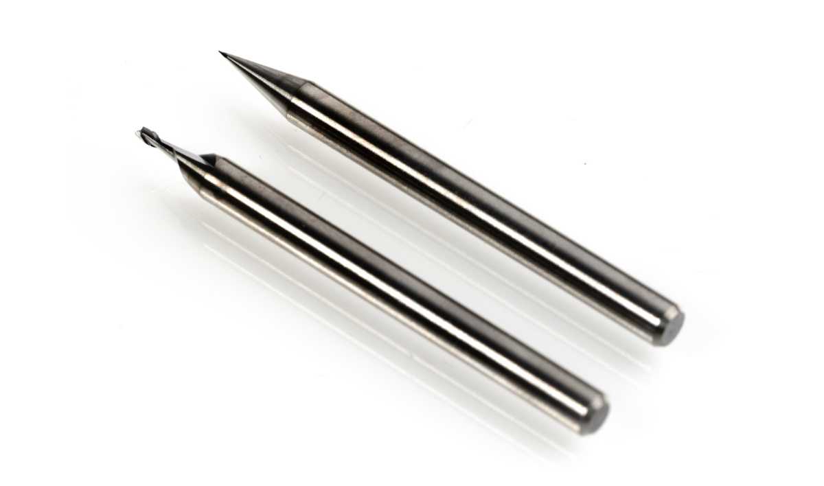
1 mm and 100 μm diameter end mill, side by side.
Challenge 2: Friction
An important factor in the molding process is that as a thermoplastic material cools, it shrinks onto the mold. The shrinking effect creates friction between the finished part and the mold, which must be overcome to remove the part during ejection.
A key to success in molding is to reduce this friction by adding a slight angle — draft — to all vertical surfaces. Draft will help to ensure that the part releases immediately from the mold during ejection instead of dragging along vertical walls, which can lead to feature damage, surface defects, and broken parts.
Design Guide link to Design Guide section
Most design constraints for the transition molding process are based on the two challenges listed above. If your design accommodates practical cutting tool diameters and you design your features to properly release from the mold, you are well on your way to a manufacturable device!
Visit the Design Guide to dig deeper into the best practices and guidelines for every aspect of transition molding.
Design feedback link to Design feedback section
Providing feedback is a core part of our process here at Parallel. We’ll check your device to make sure that it complies with best practices and suggest changes that may be necessary to ensure the success of your design. Upload your design today to receive a configurable quote that will allow you to adjust materials, configuration, quantities, and lead time on the fly.