Upload
Home
3D printing vs Machining vs Transition Molding
By Joshua Gomes
A head-to-head comparison of prototyping techniques for microfluidics.
Introduction link to Introduction section
Deciding on a prototyping technique is one of the first steps in the microfluidic development process. With several options available, it can be difficult to know which to choose based on specs alone. In this deep dive, we’ll produce a sample device with common microfluidic features using three different manufacturing processes: 3D printing, machining, and Transition Molding. Then, we’ll compare the qualitative and quantitative results to demonstrate the strengths and weaknesses of each fabrication method.
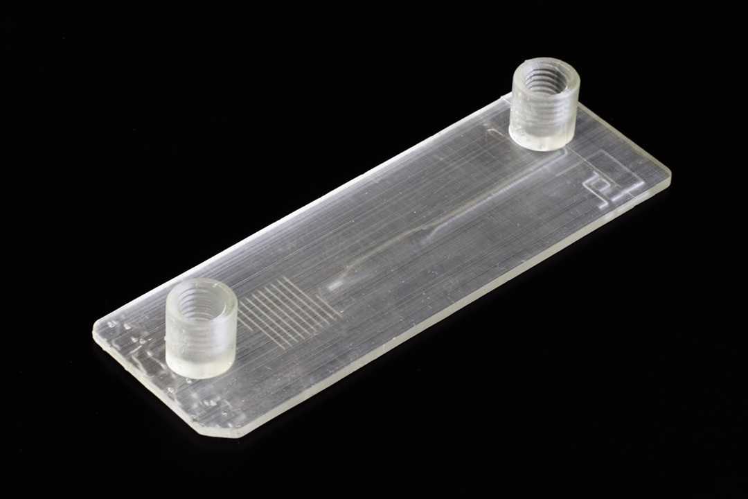
A 3D printed microfluidic device.
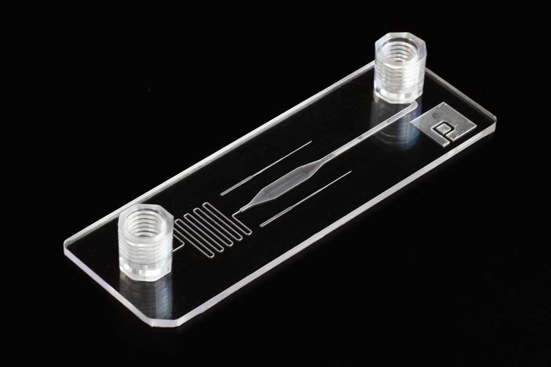
A machined microfluidic device.
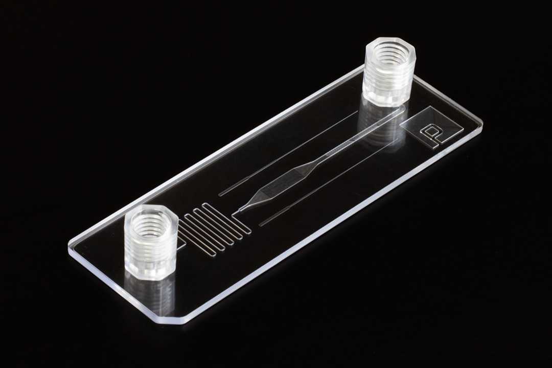
A Transition Molded microfluidic device.
What about PDMS?
PDMS (polydimethylsiloxane) is the most common material used in the academic community to prototype microfluidic devices. It is a two-component liquid silicone rubber that can be easily poured onto a master mold and cured to replicate microfeatures, yielding a soft, rubber device that can be adhered to a glass slide to seal the channels. While it is a great technique for certain applications and can produce extremely high-resolution microstructures, the material itself has several drawbacks that limit its usefulness and scalability for commercial applications. For example, PDMS binds to small molecules like drugs and reagents, decreasing the intended concentration and making experimental learnings meaningless. To that end, the NIH has advised against proposing PDMS in grant submissions for organ chips. We’ll focus on techniques in this whitepaper that more effectively reflect the desired properties of a commercial product.
Device architecture link to Device architecture section
Let’s start by reviewing a typical architecture for a microfluidic device:
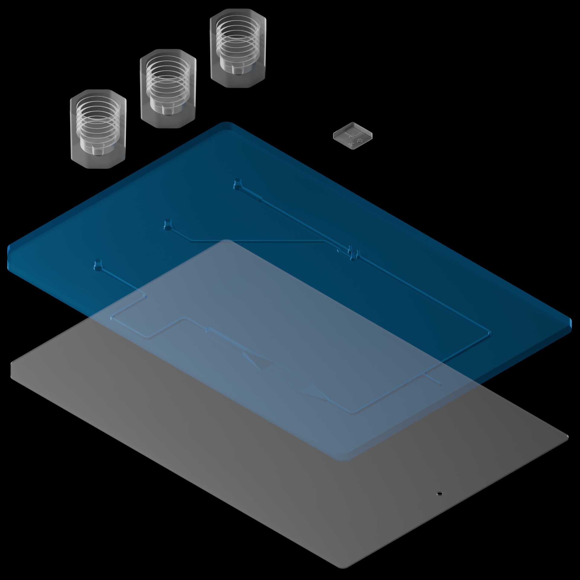
Exploded view
The heart of the device is the fluidic layer. It contains microfeatures and geometry that allow the device to perform its desired function. The accuracy, repeatability, and surface finish of the microfeatures all have a big impact on device performance.
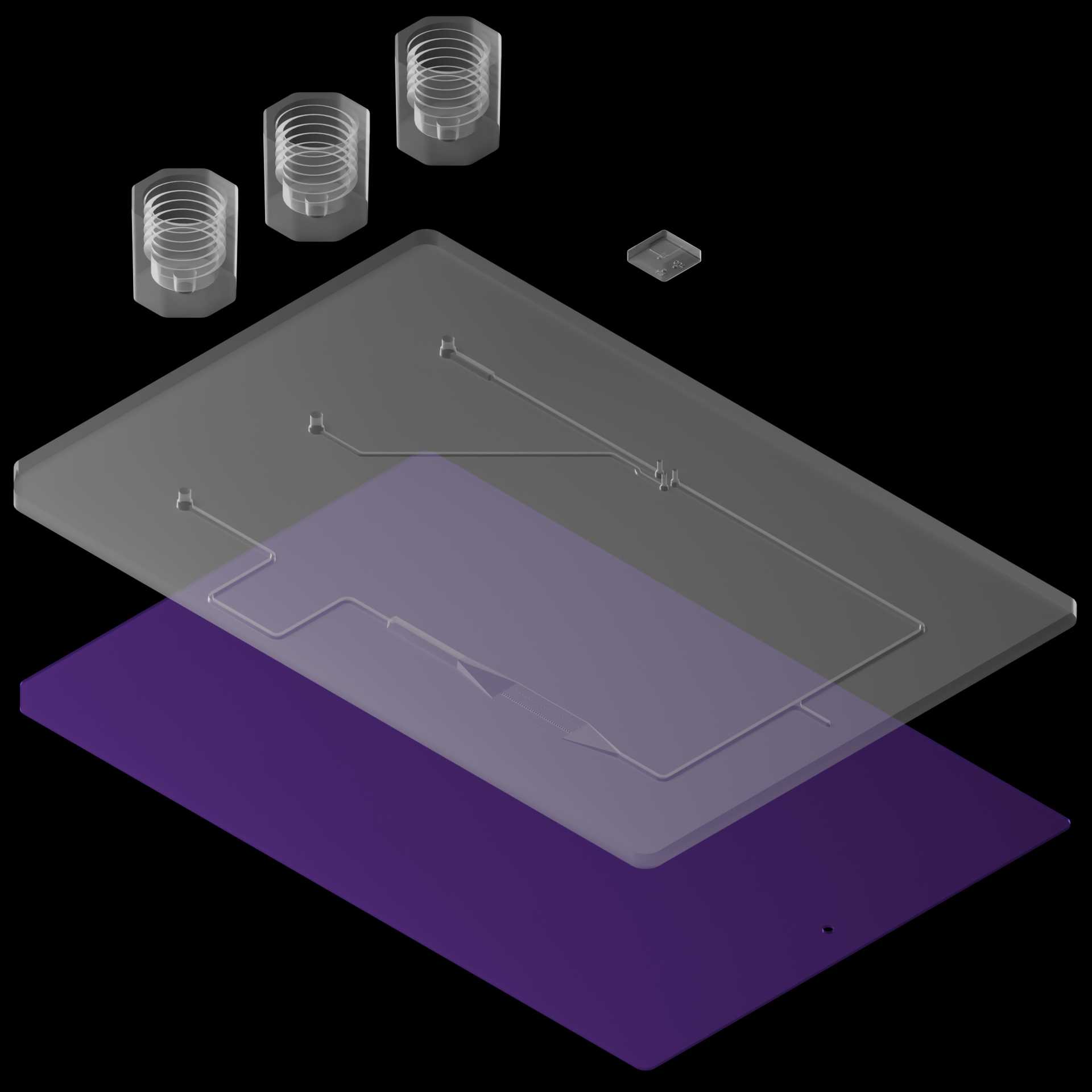
Exploded view
A cap is then used to seal the fluidic layer and form an enclosed channel that can be used to create flow. Often, imaging will be conducted through the cap layer, so optical clarity and thickness can be important considerations.
Exploded view
Finally, hardware are attached to the device that allow it to interface with the external lab instrumentation like pumps, pipetting systems, or sensors. Hardware can be added to the device as a secondary process or produced simultaneously along with the fluidic layer, depending on the fabrication technique.
Devices can vary from this architecture, especially as complexity increases. However, the simple structure we have here forms the basis of many microfluidic applications and is a good metric by which we can test different prototyping techniques.
Prototyping techniques link to Prototyping techniques section
In the following sections, we’ll discuss the most common prototyping methods for microfluidic development. If you already have a strong understanding of how each of the processes works, you may want to skip straight to the comparison section.
Fluidic layer fabrication link to Fluidic layer fabrication section
The first step in the prototyping process is to build a fluidic layer that contains all of the channels and microfeatures necessary for your application. The processes below highlight some of the most common techniques used in microfluidic device fabrication.
3D printing / Additive manufacturing
3D printing has become synonymous with rapid prototyping in engineering. It is a game-changer to create a CAD model, throw it in a printer overnight, and test your prototype the next day. The flexibility and ease of use of 3D printers are a double-edged sword when it comes to prototyping, though. A fundamental idea in the process is that a prototype should be representative of the final form of a particular concept. Sometimes the flexibility of 3D printing can cause engineers to design components that are only manufacturable by 3D printing, preventing the transition to higher volume techniques, like injection molding, without a substantial redesign. However, as long as this pitfall can be avoided, 3D printing is an excellent tool in any engineer’s kit. Several 3D printing methods are commonly used, each with its advantages and disadvantages.
FDM - Fused Deposition Modeling
When most people think of 3D printers, FDM is what comes to mind. These printers work by forcing a solid thermoplastic wire through a heated nozzle to create a molten “bead” of plastic, similar to the common hot-glue gun. The molten plastic is brought into contact with a build platform, then dispensed precisely while moving the print head in the X and Y plane to create desired geometry, forming one layer or “slice” of the 3D model. After the slice is finished, the printer will move the build platform up by the height of the next layer and repeat the process until the full model is complete.
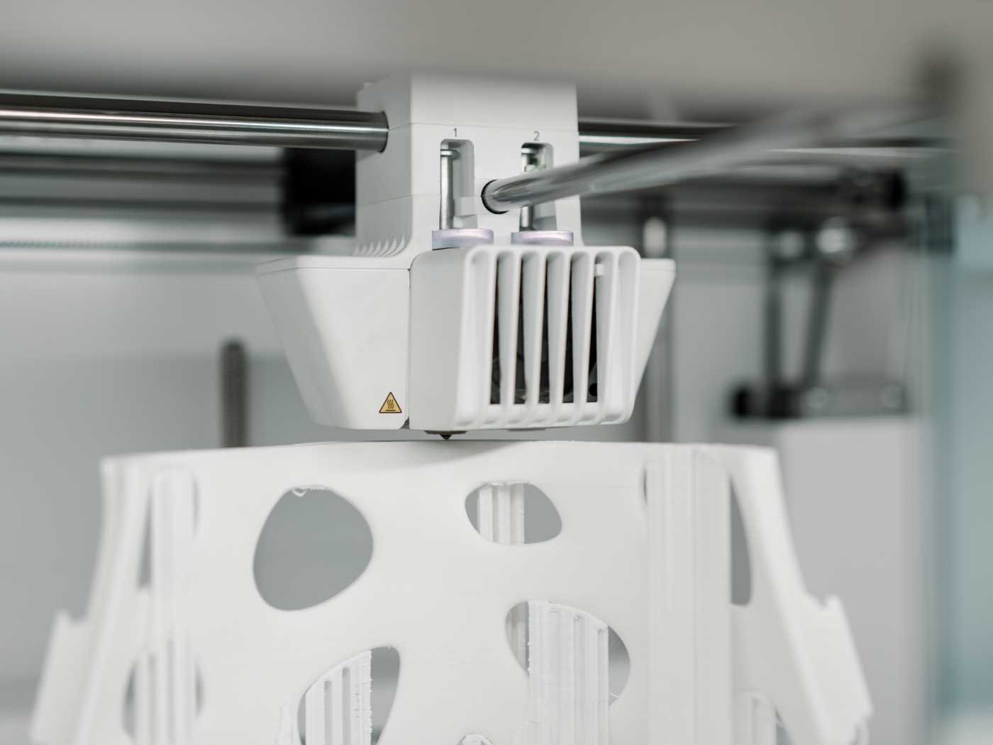
FDM 3D printer.
FDM is a relatively fast, easy method to produce mechanical prototypes. We use our FDM printer frequently to print things like jigs, fixtures, and other components. However, for producing microfluidic devices, the technique has a couple of critical flaws. First, the nature of laying down material one bead at a time creates microscopic gaps and weak points between layers. Without some sort of secondary finish step, parts produced by FDM are not liquid-tight, rendering them useless for fluidic applications. Additionally, it is impossible to produce optically clear FDM parts without significant post-processing. Together, these limitations hinder FDM’s usefulness for microfluidic projects.
Vat polymerization
3D printing by a vat polymerization is quite different from FDM techniques. Instead of relying on solid plastic wire as a feed material, liquid resin is contained in a tank or reservoir. The liquid resin, known as a photopolymer, transforms from liquid to solid when exposed to a particular wavelength of UV light. The basic build technique remains the same. A single layer of a part is exposed to a precise pattern of UV light, curing one slice of the final product. Then, the build platform translates a small amount in the vertical direction, and another slice is added layer by layer until the entire part is formed.
A key aspect of this process is constraining the light so it only interacts with the polymer in areas that need to be cured. Examples of different techniques include stereolithography (SLA) and digital light processing (DLP). In SLA printers, a scanning system, typically composed of mirrors, galvanometers, and other optical components, is used to direct a laser precisely where the desired part geometry is. DLP printers, on the other hand, use a projector to instantaneously cure an entire layer of material at one time by digitally controlling which pixels are activated.
For rapid prototyping in microfluidic applications, vat polymerization techniques have some big advantages over FDM. First, the curing method allows the devices to be liquid-tight, without the tiny micro gaps and voids that can be present in FDM systems. Also, both DLP and SLA systems tend to have higher resolution than FDM systems. Clear materials are an option, though they generally require post-processing to become fully transparent.
When evaluating vat polymerization, it's important to consider material properties. The photopolymers used in DLP and SLA systems can cause issues for fluidic applications, such as high levels of autofluorescence or poor biological and chemical compatibility. This autofluorescence effect is noticeable when parts are placed in the UV curing oven, as demonstrated by our test devices below:
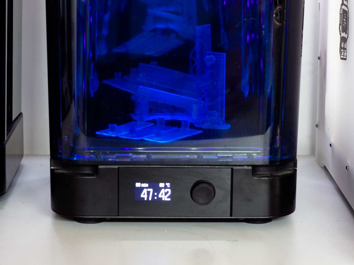
Microfluidic devices in a SLA UV curing oven.
Also, since 3D printing isn’t viable (as of today) for high-volume manufacturing, developers often need to redesign their devices for techniques like injection molding when they are ready to scale up production. Switching from UV-cured photopolymers to the thermoplastic materials used in molding can lead to major performance changes in a device. The variability introduced makes jumping straight from 3D printing to injection molding a high-risk scenario, threatening months of lead time and the large capital investment required for injection mold fabrication and setup.
Machining
Milling is a foundational process in mechanical engineering. In some ways, it is the inverse of 3D printing. Instead of adding material layer by layer, we start with a solid piece of material, or “stock”, and then use a computer-controlled machine to selectively remove material with rotating cutting tools. It is a technique that can be used to make parts the size of a school bus or, in the case of microfluidics, features that are measured in microns. Here at Parallel, our milling machine is running constantly to make microfluidic devices, tooling, and all sorts of other parts, as shown below:
CNC milling a microfluidic device.
The most common cutting tool, an end mill, is similar to the common drill bit, except it is generally flat, rather than pointed, and is designed to cut horizontally, in addition to vertically. One of the defining features of micromilling is that the cutting tools used are very small. At Parallel, we regularly run end mills as small as 100 microns in diameter, roughly the same width as human hair. To effectively mill a negative feature, like a channel or a hole, we need to be able to fit the cutting tool inside the feature. This requirement is what defines the lower limit of feature sizes that we can produce by micromilling.
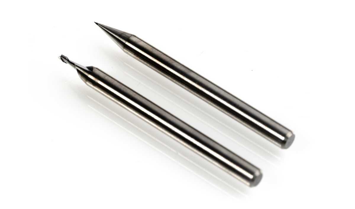
1 mm and 100 μm diameter end mill, side by side.
Micromilling is useful for microfluidic prototyping because we can produce devices from the same materials, thermoplastics, that could eventually be used in mass production. This helps to ensure that prototypes will be representative of the performance that we will see in the final product. Additionally, micromilling can be a great way to produce one or two parts. No mold is required, and a single prototype may only take up to an hour of machine time, depending on complexity. One drawback is that it requires a skilled machinist to effectively deliver a part that will meet the tolerances required in most microfluidic applications. Also, a competent micromilling machine will often cost more than $100,000.
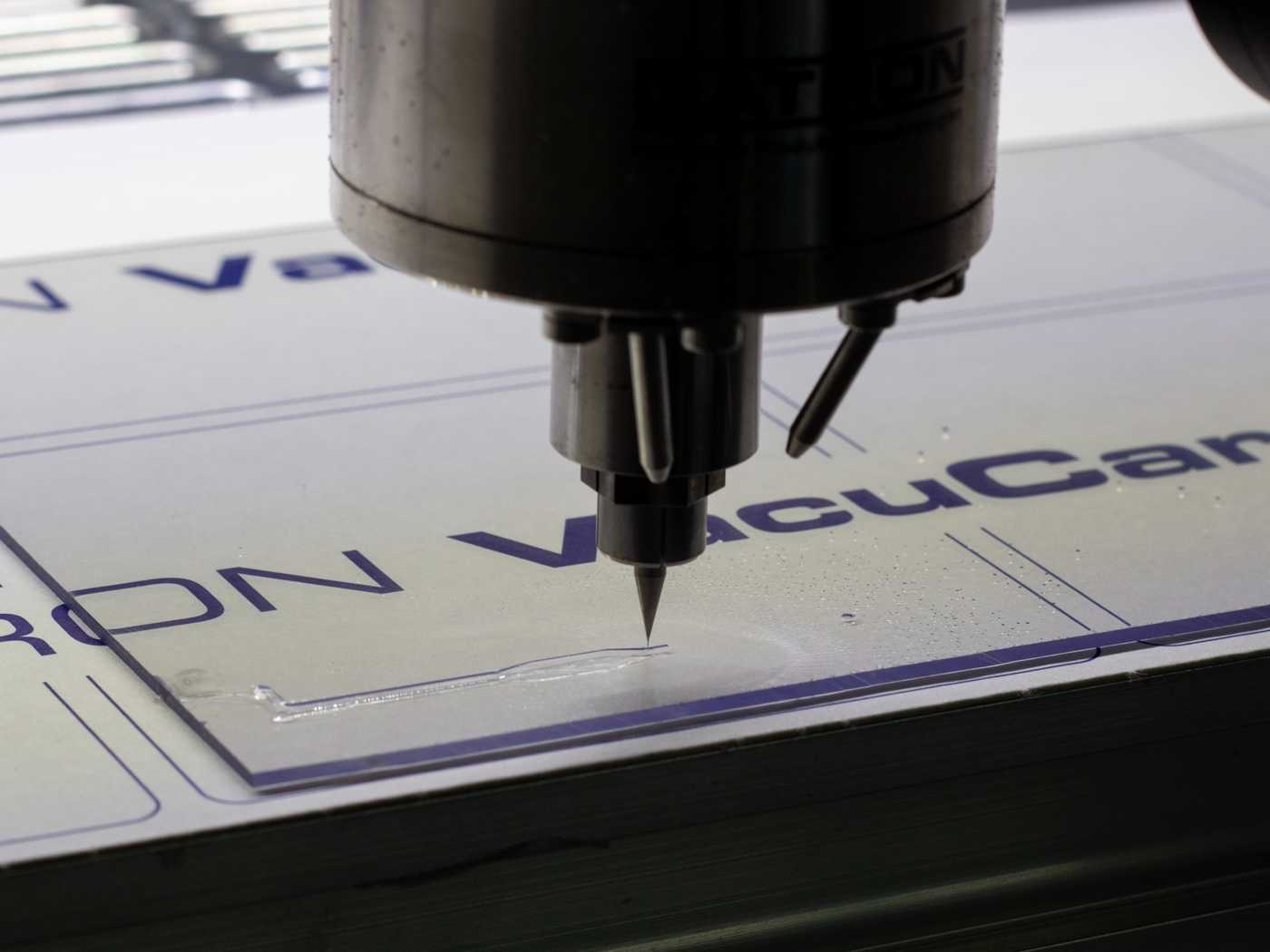
Transition Molding
The most frequent method we use here at Parallel to create microfluidic prototypes is Transition Molding. The first step in the process is to create an aluminum mold, sometimes called a master, with the inverse of your desired feature geometry. For example, if you designed a fluidic layer with small recessed channels, the mold would require proud aluminum features of the same size. The mold is then placed in our Transition Molder, where we form molten thermoplastic resin against the geometry of the mold, allowing it to replicate the microfeatures. The plastic then cools, solidifies, and is ejected from the molder as a fully formed fluidic layer.
Capping link to Capping section
Capping, otherwise known as sealing or lidding, is the process of bonding a cap to the fluidic layer to create fully sealed channels.
Pressure-sensitive adhesive
PSA films are an inexpensive and easy method to cap devices. They are essentially single-sided tape with specially chosen adhesives to match particular applications. Adhesives Research and 3M are two of the leading manufacturers of PSA films designed for microfluidics applications. The assembly method for these films is typically easy enough to accomplish in most lab or engineering environments, maybe with a bit of rolling or clamping in a press to make sure the adhesive forms a good bond. The straightforward assembly can help to keep the costs of prototyping low.
When using PSA, there are some things to keep in mind. First, the adhesive will be in direct contact with the liquid flow path. Adhesives exposed to such small flows can often create problems in sensitive applications. It is also possible to either obstruct channels or deform adhesive into the microfeatures, changing their geometry. For many single-use diagnostic applications, adhesive films can be a great choice. However, adhesives are usually a non-starter for the most demanding applications, especially when small molecules are involved. From a flexibility standpoint, though, PSAs are compatible with all three prototyping methods discussed so far and are easy to implement in mass production.
Laser welding
In laser welding, concentrated light is directed at the joint between two materials, locally melting plastic at a “weld joint.” First, the two parts to be joined are clamped tightly together. Typically, one of the parts (i.e. the fluidic layer) is absorptive to infrared radiation, and the mating part (i.e. the cap) is transmissive. An infrared laser will then trace the outline where the parts should be welded, either using a mask or precise motion control to direct the beam. The absorptive layer will locally melt when exposed to laser energy, eventually melting and forming a strong bond with the transmissive layer.
Laser welding is a powerful process that doesn’t require any adhesive. However, it lacks the accessibility of the PSA approach. Generally, the cap and the fluidic layer must either be the same material or chemically compatible. Also, since one of the layers needs to be absorptive, one of the parts must contain an IR-absorbing additive. While this may be perfectly acceptable in some applications, many require that all device layers be transmissive to enable imaging. Other welding techniques use a 2-micron wavelength laser source, which is partially absorbed by transparent polymers. In some instances, this can allow for a laser joint without additives. However, the risk of feature deformation, especially for small features, becomes problematic with this approach.
Solvent bonding
Solvent bonding offers a way to attach a cap and fluidic layer made of the same material without any adhesive. In this case, a solvent is applied to both surfaces to be bonded either in gaseous or liquid form. Then, the two parts are firmly clamped together until the solvent evaporates. Heat and pressure may be added to assist in the bonding process.
This technique can produce strong bonds, but it creates a risk of deforming channel features. Also, the solvents required to dissolve some polymers used in microfluidics can be quite hazardous. For these reasons, we avoid solvent bonding here at Parallel.
Thermal diffusion bonding
In thermal diffusion bonding, the two layers are heated to just below their glass transition temperature, where the material changes from a glassy state to a rubbery state. Then, they are firmly compressed together to create a seal. When done correctly, this allows a strong bond between parts made from the same type of plastic without the risk of major channel deformation. It, too, lacks the flexibility of PSAs because you are forced to use chemically compatible materials for each layer. However, the advantages of being adhesive-free, fully transparent, and solvent-free make it an attractive option for many applications. Thermal diffusion bonding is the typical method that we use here at Parallel Fluidics to cap devices.
Prototyping method comparison link to Prototyping method comparison section
Instead of presenting only the trade-offs of the different methods in generalities, we thought it would be more informative to produce the same device with the different prototyping techniques and compare the results. We’ll use a sample part to demonstrate some of the most common feature requests our customers require for their applications. The design can be seen in the CAD model below:
Sample device features
Inlet serpentine
Serpentine channels are often used to fit long channel lengths into compact areas. In our sample device, we have a 150 micron by 150 micron serpentine that leads from the inlet port to the other features in the device.
Capillary valve
The next microfeature is called a capillary valve. It is designed with a sharp increase in channel height and width so the liquid flow front is forced to experience a rapid expansion. The surface tension of the liquid will resist the expansion, stopping the flow until a critical amount of pressure is reached. Capillary valves can be found in many applications, such as sample collection, volume metering, and centrifugal microfluidics.
Tapered channel
Many applications require smoothly tapering surfaces from one channel height to another. Gently tapering features with a good surface finish can help prevent bubbles from being trapped during use.
Herringbone mixer
Channel features are typically small enough in microfluidics to ensure that devices will always operate in a laminar flow regime. This phenomenon is critical to the success of many different microfluidic devices, such as droplet generators and cell sorters. However, sometimes you may want to induce turbulence, like when attempting to mix two different inlet fluids completely. A herringbone mixer consists of a series of recesses in the bottom of a microfluidic channel that is designed to achieve this effect.
Ports
Most microfluidic devices need to be connected to an external flow source. In this sample design, we’ll include ¼-28 threaded ports designed to work with capillary tube fittings.
Stepdown channel
The stepdown channel has a consistent height of 50 microns but varies in width from 500 to 50 microns. It will be used to evaluate the dimensional accuracy of the different prototyping techniques.
We’ll produce this device using the three methods we most frequently use in-house here at Parallel Fluidics: 3D printing, micromilling, and Transition Molding. We’ll evaluate the features qualitatively using the microscope setup pictured below and take quantitative channel measurements with our optical coordinate measuring system.
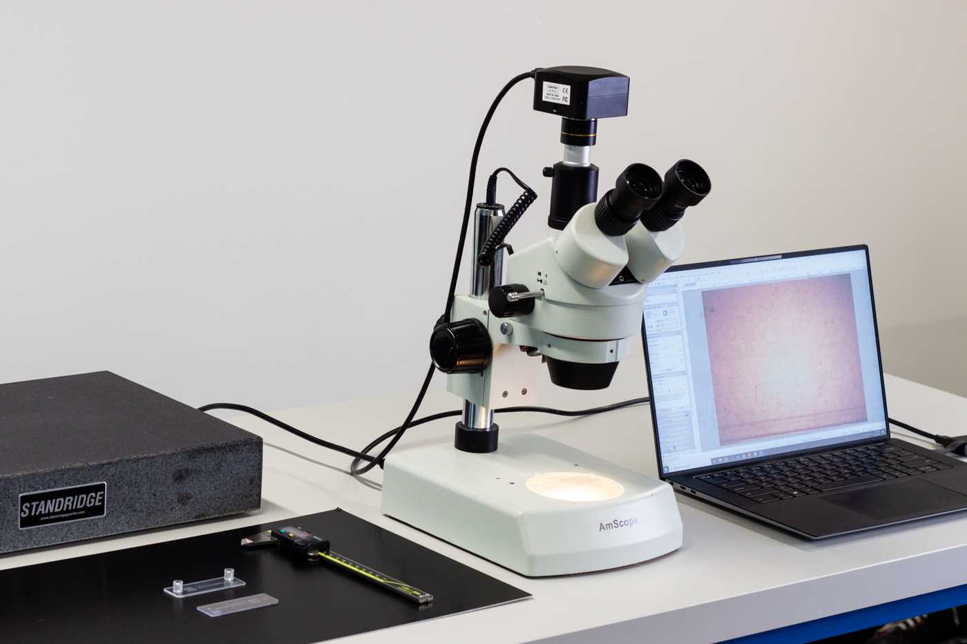
Microscope setup used for inspecting microfluidic prototypes.
Comparison: Macro impression link to Comparison: Macro impression section
3D printing
- Machine used
- Formlabs Form 3
- Material
- Clear resin V4
- Capping method
- Uncapped
- Ports
- Printed in place
The first impression of the 3D printed device is that it is much less transparent than the other devices, with noticeable build lines from the printing process and an overall yellow hue. We tried printing in a few different orientations to minimize the effect, but found that the results were all similar. There is a significant warp across the length of the device, which seemed to develop during the post-curing process. There are also still some remnants from the printing supports that would need sanding or other post-processing to smooth out. The larger sections of the microfluidic channel are visible, but even by eye, it’s fairly obvious that the small microfeatures didn’t replicate effectively. The outer dimensions of the device and the ¼-28 ports seemed to print well.
Micromilling
- Machine used
- Parallel Fluidics High Speed Vertical Machining Center
- Material
- Polycarbonate
- Capping method
- Pressure sensitive adhesive film
- Ports
- Parallel Fluidics ¼-28 port
The micromilled device is much more transparent than the 3D printed device at first glance. The sections of the device that don’t have microstructures are extremely clear, while the channel floors obviously have a more hazy surface. There are some minor scratches on the cap, but otherwise, it is nice and flat when viewed under a bright light. The device doesn’t have any noticeable warp, and the ¼-28 ports are well attached. The microfeatures look like they were reproduced well by eye, with the caveat that we weren’t able to mill the smallest sections of the stepdown channel due to the minimum end mill diameter.
Transition Molding
- Machine used
- Parallel Fluidics Transition Molder
- Material
- Polycarbonate
- Capping method
- Thermal diffusion bond
- Ports
- Parallel Fluidics ¼-28 port
The macro impression of the Transition Molded device is similar to the milled prototype. Overall, the device is quite transparent, and the channel floor has the least haze of the group. The most obvious difference from the others is the stepdown channel extends further along the device because we were able to produce the full range of channel widths.
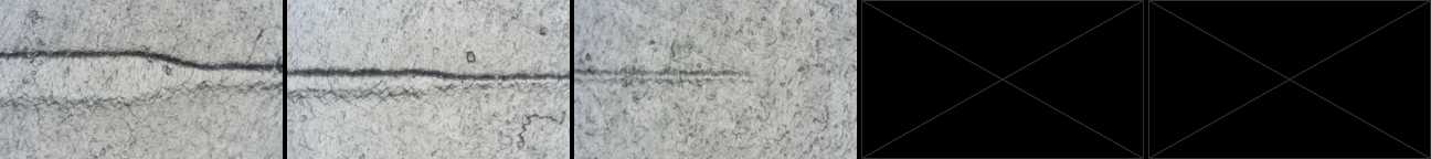
Comparison: Inlet channel, capillary valve, and tapered surface link to Comparison: Inlet channel, capillary valve, and tapered surface section
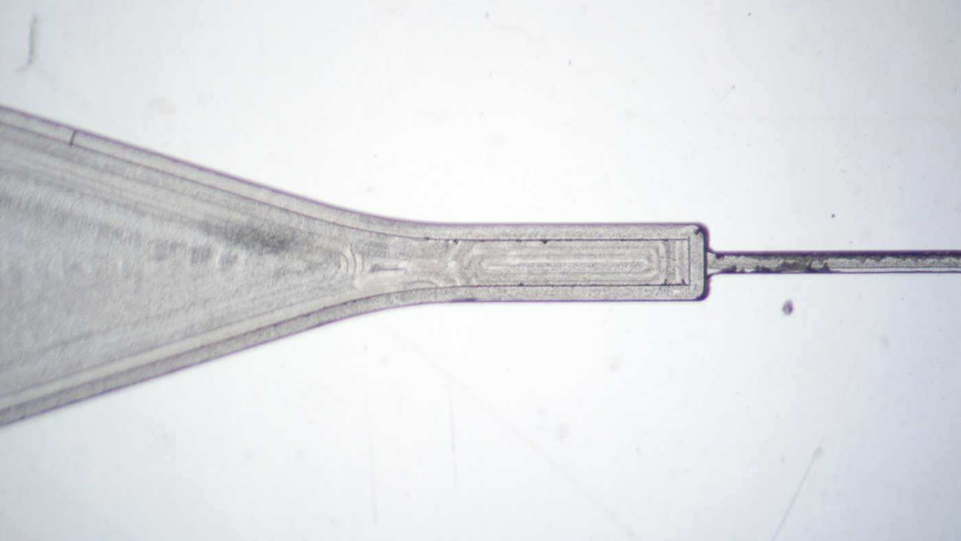
3D Printing
3D printed capillary valve and sloped microfluidic channel.
The 3D printed features are somewhat present, but the printing process could not reproduce the smaller channel for its entire length, and the capillary valve is missing entirely. The transition from the channel floor to the top surface of the device is rounded and inconsistent. The surface is also quite textured under the microscope, with an almost melted appearance.
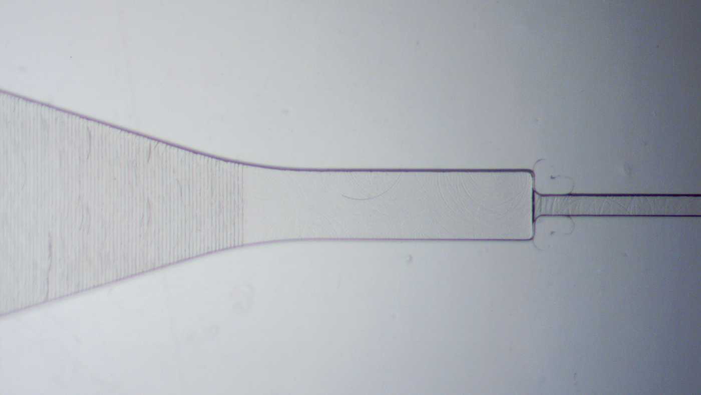
Micromilling
Micromilled polycarbonate capillary valve and sloped channel.
The milled device has distinct features with very defined edges, a major improvement over the 3D printed device. It is transparent outside of the channel, but the channel floor shows obvious roughness from the milling process, which gives it an opaque appearance. There are large burrs obstructing the smaller channel and smaller burrs at the bottom of the larger features, even though the part was washed in an ultrasonic bath after machining. Otherwise, the geometry looks as intended. The sloped section of the channel seems to vary evenly, transitioning from the 250 micron to the 100 micron depth.
Transition Molding
Transition Molded polycarbonate capillary valve and sloped channel.
The geometry in the Transition Molded version looks qualitatively close to the intended design. Compared to the other methods, the channel floor is much more transparent, without the burr and particulate issues present in the machined device. There are still some faint toolmarks that are noticeable in both the flat and sloped channel floors.
Comparison: Herringbone mixer link to Comparison: Herringbone mixer section
3D printing
A 3D printed microfluidic channel with a herringbone mixer.
The channel is present, but the printing process did not effectively reproduce the internal herringbone features. We can see distinct horizontal and vertical lines both parallel and perpendicular to the build direction of the printer.
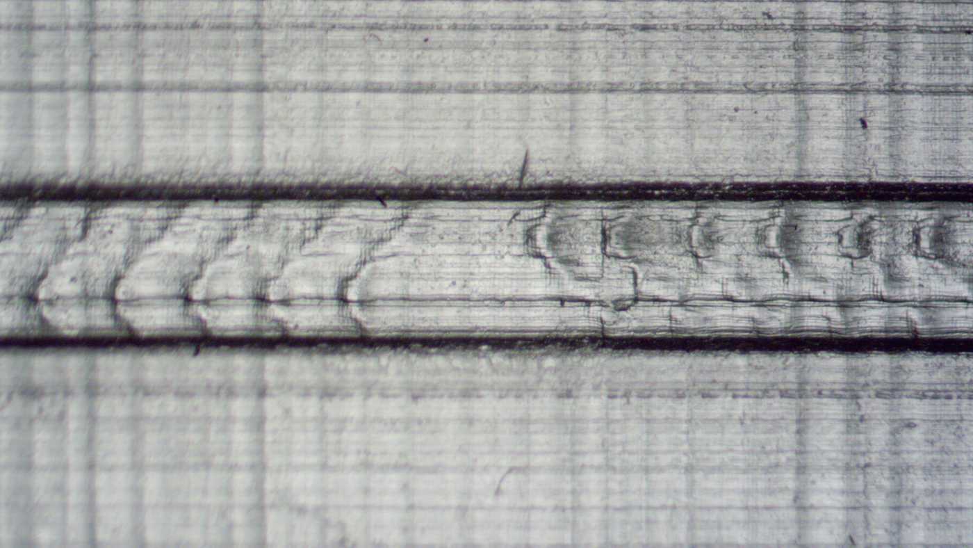
Micromilling
A micromilled microfluidic channel with a herringbone mixer.
The geometry of the milled herringbone mixer looks close to the intended geometry. However, there are obvious burrs around the edge of each of the herringbone pockets. Burrs like these can be a challenge for fluidic applications because they can disrupt flow, lead to problems with wetting the channel effectively, and trap cells or particles.
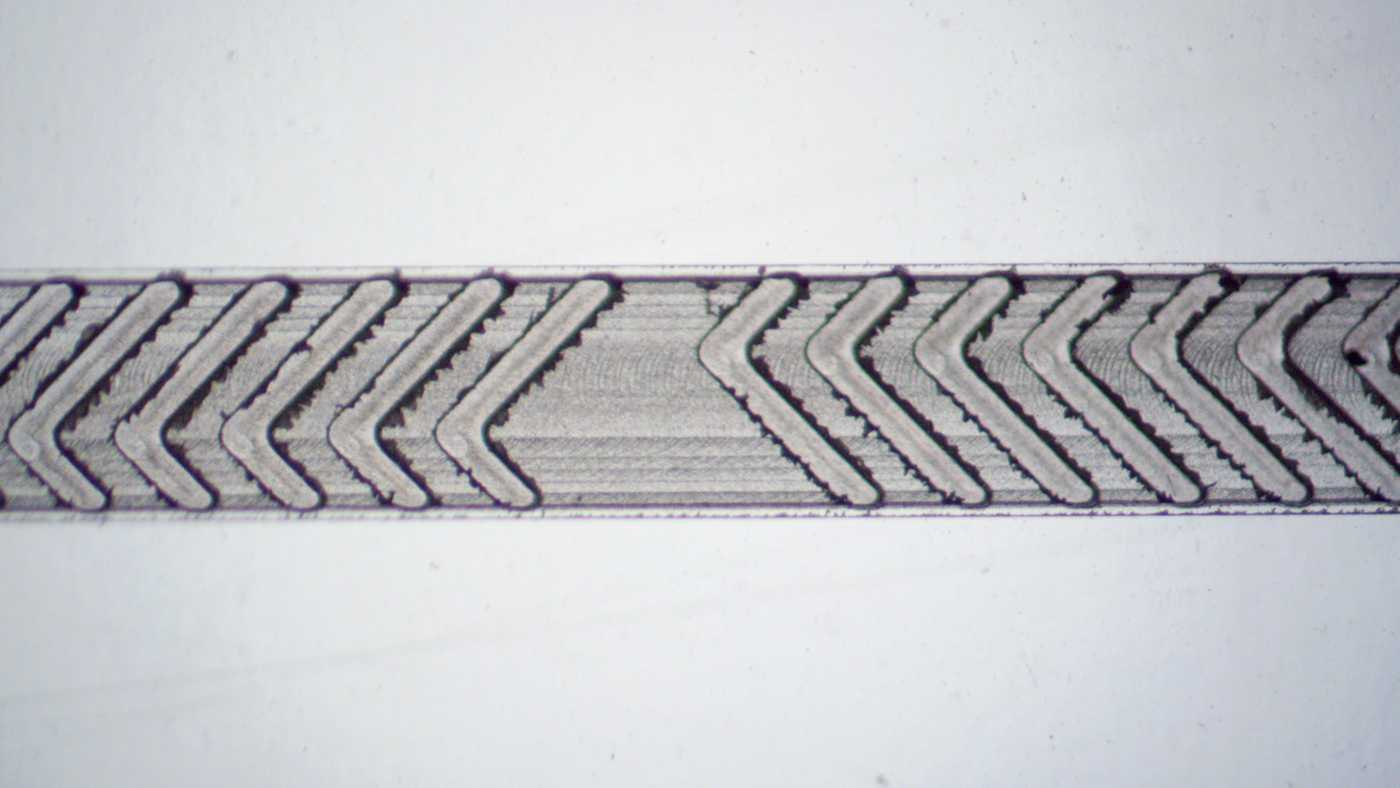
Transition Molding
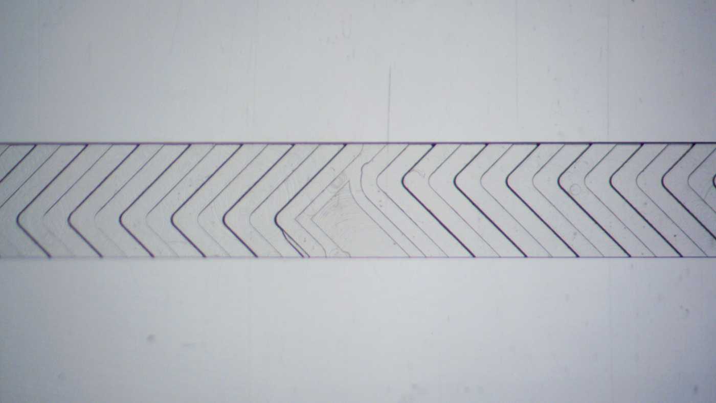
A Transition Molded microfluidic channel with a herringbone mixer.
The channel surface here is again the clearest of the bunch, but there are still some faint tool marks at the bottom of the features. The geometry looks as intended, and the channel edges are crisp and clean, without any noticeable burring or particulate.
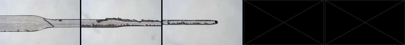
Comparison: Stepdown channel link to Comparison: Stepdown channel section
3D printing
A 3D printed microfluidic channel that steps down from 500 microns to 150 microns.
The stepdown channel is visible in the 3D printed prototype at its widest section. However, in the 150 micron width region, it tapers away to nothing. Otherwise, the results are similar to the previously described 3D printed features, with an even more noticeable rough surface in these higher magnification photos.
Micromilling
A micromilled polycarbonate microfluidic channel that steps down from 500 microns to 150 microns.
There are a lot of burrs, particularly in the smallest section of the channel. The smallest width channel that we were able to produce was 150 microns due to the lower limit of end mill diameter that we can effectively run on our milling machine
Transition Molding
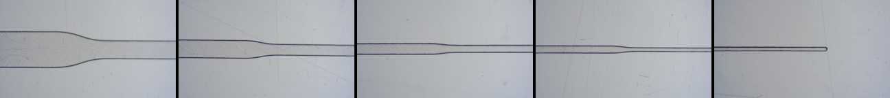
A Transition Molded polycarbonate microfluidic channel that steps down from 500 microns to 50 microns.
In the transition molded prototyped, we were able to reproduce the stepdown channel down to the minimum width of 50 microns. The channel floor still has some faint tool marks. It again doesn’t show any noticeable burrs or particulate, even down to the smallest channel.
Comparison: Measurements link to Comparison: Measurements section
In addition to the qualitative observations from the stereoscope, we also inspected devices for accuracy with our Optical Coordinate Measurement Machine (CMM). This device allows us to capture very precise measurements of channel dimensions in X, Y, and Z. This data was all captured prior to capping the devices in order to make the measurement process easier.
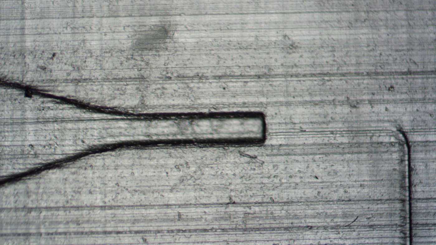
3D printed channel
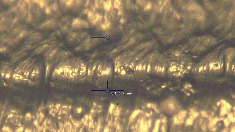
Optical width measurement of a 3D printed channel designed at 150 microns.
| Measurement | Designed | Measured | Delta |
|---|---|---|---|
| Width | 150 microns | ~100 microns | ~50 microns |
| Height | 50 microns | ~25 microns | ~25 microns |
Micromilled channel
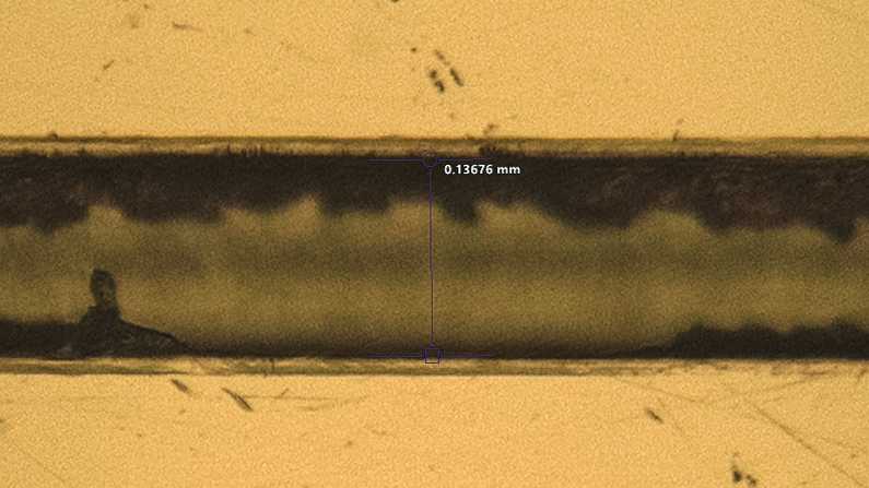
Optical width measurement of a micromilled channel designed at 150 microns.
| Measurement | Designed | Measured | Delta |
|---|---|---|---|
| Width | 150 microns | 137 microns | 13 microns |
| Height | 50 microns | 54 microns | 4 microns |
Transition Molded channel
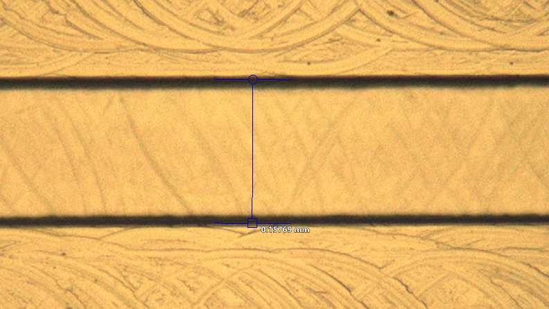
Optical width measurement of a Transition Molded channel designed at 150 microns
| Measurement | Designed | Measured | Delta |
|---|---|---|---|
| Width | 150 microns | 158 microns | 8 microns |
| Height | 50 microns | 46 microns | 4 microns |
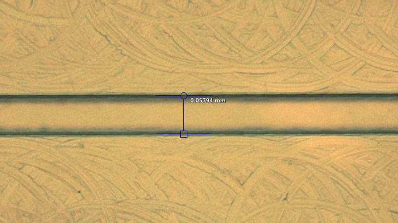
Optical width measurement of a Transition Molded channel designed at 50 microns.
| Measurement | Designed | Measured | Delta |
|---|---|---|---|
| Width | 50 microns | 58 microns | 8 microns |
| Height | 50 microns | 46 microns | 4 microns |
Our quantitative measurements confirmed that SLA printing isn’t viable for the feature sizes and accuracy needed for this device. The micromilled channel fared well dimensionally, with fewer than 15 microns of deviation in height and width for a 150 micron channel. However, it is readily apparent from a quick glance that the burrs in the channel would be problematic in a real application. Finally, Transition Molding proved very close to the nominal dimensions of the design, with fewer than 10 microns of variation. Also, it was the only process with enough resolution to produce both the 100 micron and 50 micron sections of the stepdown channel.
Summary link to Summary section
We explored the 3 different prototyping processes we use here at Parallel Fluidics. In the end, the method that you choose has to be dependent on your project's needs.
3D printing isn’t a viable strategy for this particular device with the hardware that we have at Parallel. Other systems may provide better results, but surface roughness, material compatibility issues, and lack of precision are all major challenges when using 3D printers for small microfeatures.
Micromilling can be an extremely fast way to make one or two prototypes, especially when feature sizes are relatively large and the application is simple. However, you can quickly run into problems when you need small microfeatures or smooth surfaces.
Transition Molding is our preferred method for the most demanding microfluidic projects. It leads to higher precision, better feature replication, and improved clarity over micromilled devices, while also providing a more direct representation of mass production techniques like injection molding.
Connect with our engineering team to figure out which manufacturing strategy is right for your project.